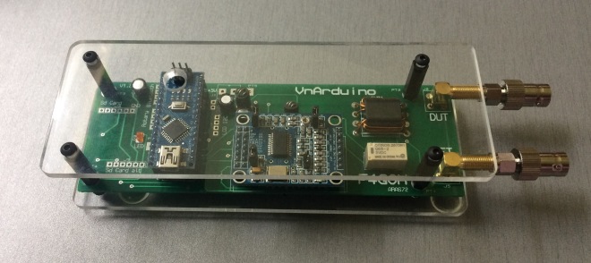
By F4GOH
The main characteristics of Vna analyzer are:
- HF : 1 MHz à 60MHz
- Reflection and transmission analysis
- Uses the DL2SBA Jvna software
- Mode « Standalone »
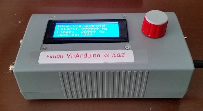
- LCD display 4 × 20
- Bluetooth with Blue VNA Androïd software
- Scrolling menu by rotary encoder
- Cost € 50 without Bluetooth Module
The VNA is based on the following components:
- Arduino NANO
- Module ad9851
- ad8302
ebay-links : components list
Pcb available mail me : f4goh@orange.fr
Introduction :
This HF VNA is an adaptation of the scheme described in the Russian site RA4NAL. I use an Arduino Nano and system measurement on the same board. I add rotary encoder and lcd display to use the VNA in standalone mode. The PC software is Jvna same as miniVna from DL2SBA.
you can use the VNA from 3 differents software interfaces:
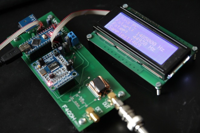
Mode 1: Connect to PC
The VNA is connected to Arduino nano via miniUSB. The PC software is Jvna same as miniVna from DL2SBA (http://vnaj.dl2sba.com).
It is possible to analyse antennas in reflection mode or filter in transmission mode.
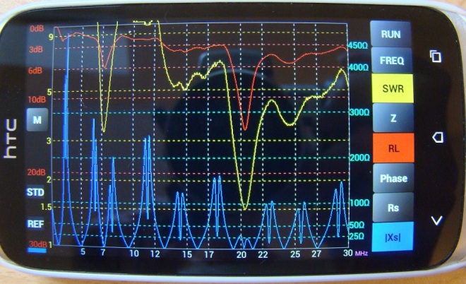
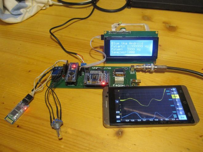
Mode 2: Connect via Bluetooth Module
The VNA is connected to via Bluetooth Module. Using blue VNA software, it is possible to analyze antenna like on PC computer, except you can up the VNA on the top of your pylon.
you can then perform analysis without cable.
(https://play.google.com/store/apps/details?id=ro.yo3ggx.btvna&hl=fr)
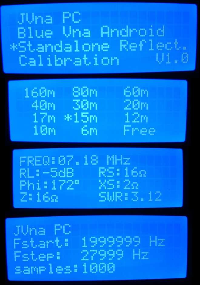
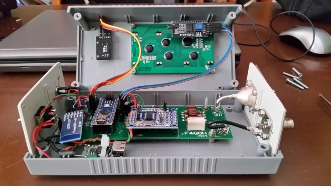
Using Mode 3 in « Standalone ». Just a 5V power supply to operate all. With mSd Card inserted, all measurements is saved in a text file. It can be possible to anayse them on a spreadsheet.
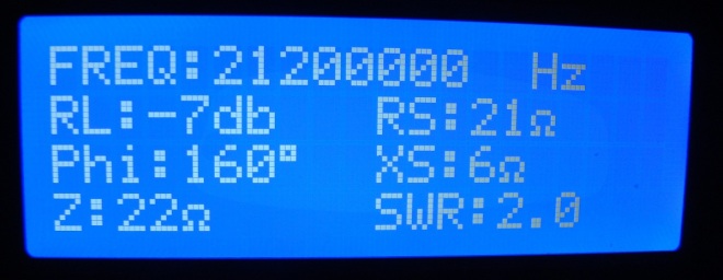
The information of antenna parameters are displayed on a 4 x 20 character LCD screen. The selection of the band or frequency is done with a rotary encoder.
the handling is quick and has few menus.
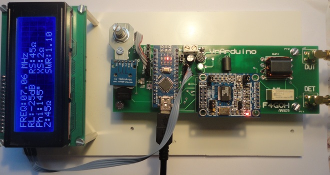
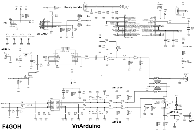
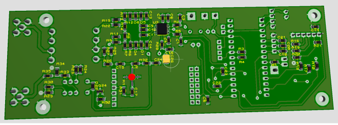
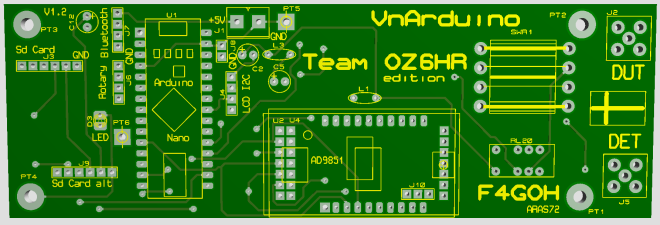
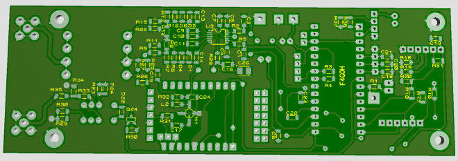
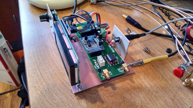
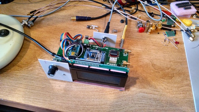
Main board description :
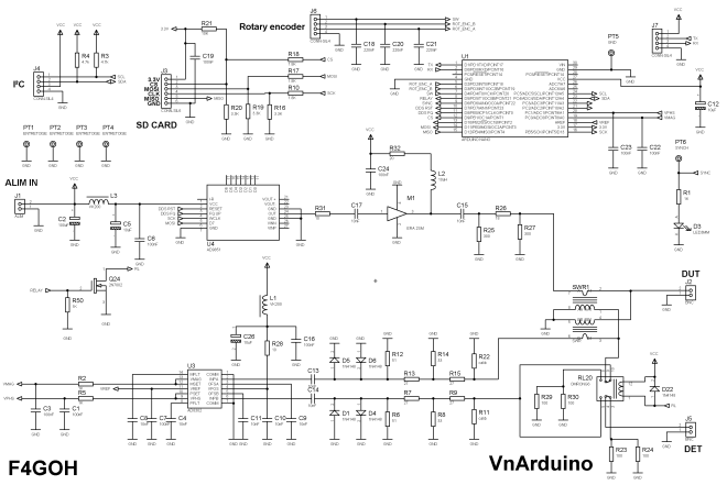
We can easily recognize the RA4NAL scheme, the Arduino UNO was replaced by a NANO facilitating the integration of the USB connection.
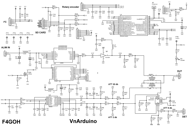
The AD9851 DDS is an oscillator, the signal is amplified by an ERA2SM and attenuated by R25,R26,R27 before attacking the tandem coupler based on a BN43-202.
The direct and reflected power of the coupler is attenuated by a couple of T Résistors and injected into a ad8302
The ad8302 will give us a DC voltage proportional to the magnitude and phase of the two signals.
These two voltages Vmag Vphs and are converted into an average of 20 digital values by the Arduino.
In PC software mode , these numericals values is directly transferred into Jvna software. Jvna compute all antenna parameters like RL, |Z|, |XS|, theta, swr.
SPI connection is shared between the DDS and the MSD card. Knowing that the power supply of the MSD card is 3.3V, it will add tension divider to Arduino.
The LCD display 24 × 20 characters is controlled via the I2C bus provided that it is equipped with a PCF8574 interface (I2C Serial Interface Module For LCD1602 Display).
Beware to use an bluetooth module (connected on J7) is compatible 5V level I / O, because this is not the case for all modules.
If you wish to scan with Jvna software on PC, you must disconnect the Bluetooth module in order not to provoke conflict on the serial line.
The LED D3 lights when there is a data transfert on the serial line.
Omron relay allows to activate the mode of transmission and thus measure the gain of a filter interposed between the DUT output and input DET.
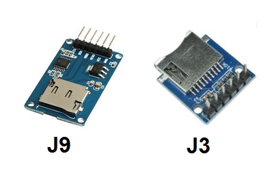
 If you want to use mSD card, you must load VnaArduinoSd.ino into Arduinonano, and install Arduino sdfat library. Insert your mSDcard into a module and connect it to J3.
Soldering and testing:
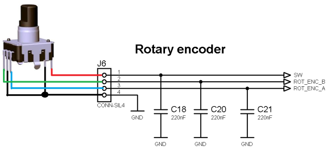
Start with soldering the support of the Arduino Nano, support for the AD9851 DDS, the connector of the LCD display and rotary encoder. (rotary.png)
Do not forget the decoupling capacitors and anti-bounce. (C12, C18, C20, C21)
VnArduino.ino program the file in Arduino from the following link:
https://github.com/f4goh/VnArduino
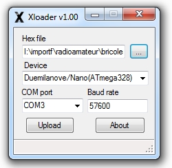
Use xloader if you want to upload firmware without compilation
Hold the rotary encoder button for switching on to access the menu.
From the menu, choose JVNA
Once validated, then the Arduino reset itself into JVna mode
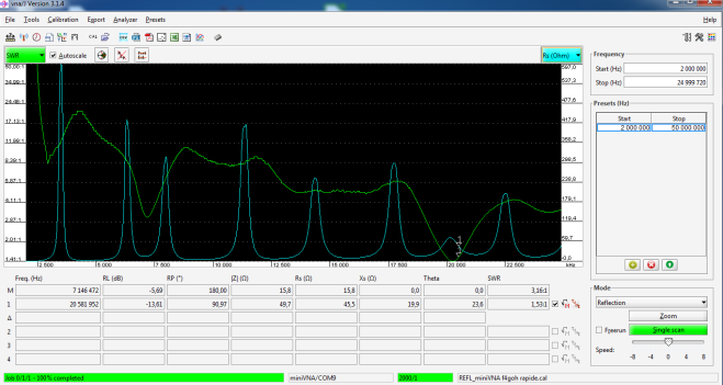
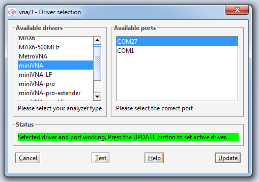
Start Jvna on your computer, choose the correct COM port in the « driver selection » menu and « miniVNA ». Make a connection test and click update.
Perform a phony reflection calibration for now, then in the frequency calibration menu adjust the DDS ticks 23,860,477 to be compatible with the AD9851.
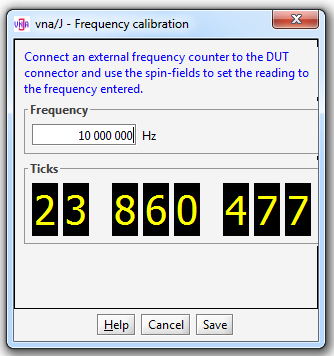
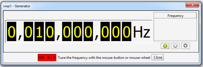
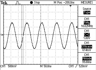
Go into the GENERATOR menu, click « on air », then check the frequency generated with an oscilloscope on the DDS output. (10Mhz) Adjust ticks to obtain 10Mhz with a frequency counter.
Solder now the ERA-2SM amplifier or an equivalent component of your stock.
Recheck the output signal of the amplifier with an oscilloscope
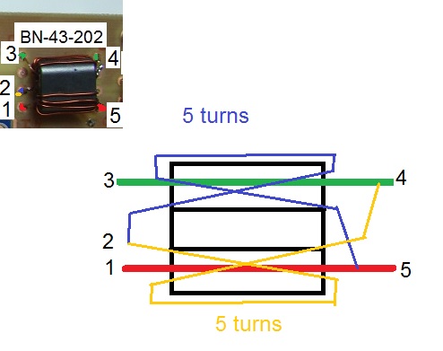
Now weld the measuring bridge (tandem coupler) and the T attenuators.
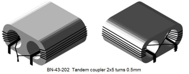
The tandem coupler used to measure the direct and reflected powers is made with a binocular toroid BN-43-202 (2×5 turns, 0.5MM)
On 50 ohm load, check with an oscilloscope the voltages across R12 (max forward voltage) and the terminals of R6 (reflected voltage near zero).
Without load (open output), with an oscilloscope check the voltages across R12 (max forward voltage) and the terminals of R6 (max reflected voltage).
Finish by weld the components around the ad8302.
Check with a voltmeter the reference voltage VREF supplied by ad8302 to be 1.8V.
The VNA is ready for use.
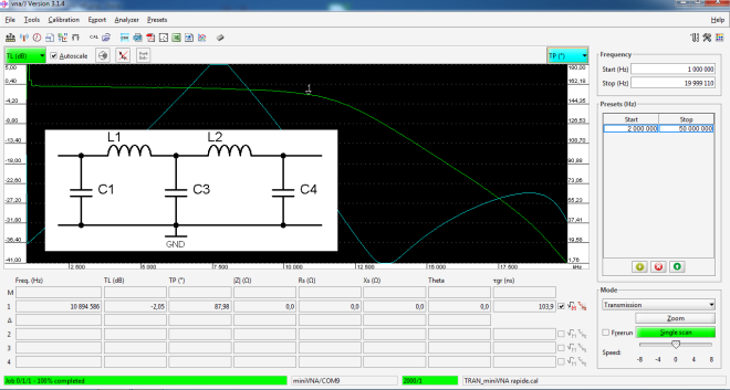
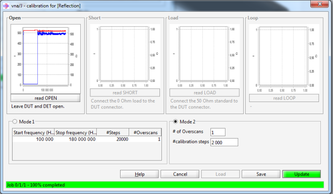
Repeat calibration, this should match the screenshot below.
 To use the « standalone » mode, it will be necessary to perform a calibration (menu on the 4th line of the LCD display).
The location of calib resistors are used to adjust the load on measurement for 50ohms RS = 50 ohm.
It is then necessary to place a single resistor with a value between 300ohms and 2Kohms on one of the two sites, but perhaps only will you not need.
73 and good parts assembly
Improvement of the measurement by F1AIA:
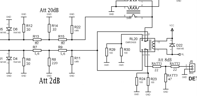
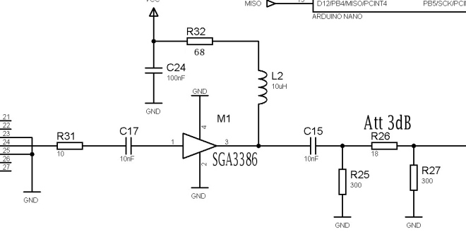
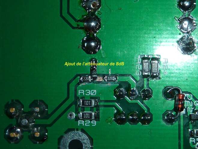
Below the diagrams containing the changes to be applied at the level of attenuation values as well as the amplification part with the replacement of a ERA to SGA3386. By applying these corrections, you can be measured attenuations to -40dB and S11 values or Return Loss (RL) -35 to-39dB.
The dynamics of the whole is enhanced with better amplification of SGA, accompanied by a better choice of reference values applied to the inputs of the AD8302.
Jean-Claude thank you for this info.
OZ6HR Edition
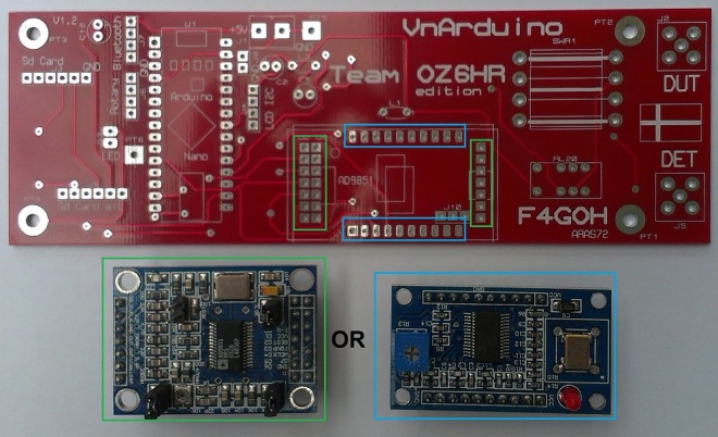
- Choose U2 or U4 depend of ad9851 pad(if you use U2 put a strap on J10 (2-3)
- For card reader choose J3 or J9 depend of sd reader (if you use J9 do not put R16 to R21and R10 resistors)
Update file on github for special OZ6HR edition
Congratulation Rainer (OE1KFR)
Thanks to YL2GVC for his picture, great !

[…] Opis i szczegóły znajdziecie na stronie projektu – LINK […]
J’aimeJ’aime
Thanks for the link to
http://ywd.pl/vna-na-arduino-i-ad9851/
73
Anthony
J’aimeJ’aime
Hello Anthony
I am going to put a VNArduino together, but wonder if the change in attenuation values,
only is to be done together with the SGA mmic amp, or could be done in all situations?
J’aimeAimé par 2 personnes
I received your circuit board yesterday – fine quality, thank-you.
J’aimeJ’aime
ebay links do not work ?
how about a different format ?
J’aimeJ’aime
Hello
I have made a contact to DL2SBA Dietmar, about the VNArduino and he has added the VNArduino with range 0,1-65Mhz
The PC software is Jvna from DL2SBA (http://vnaj.dl2sba.com).
My VNA is working ok, only thing is a not so precise encoder.
vy 73 de oz1fhu
J’aimeAimé par 1 personne
Merci bien Anthony, 73!
J’aimeJ’aime
[…] https://hamprojects.wordpress.com/2016/02/21/hf-arduino-vna-english-version/ […]
J’aimeJ’aime
I’m about to start building this project, but I’m not sure about how to find the values for calibration resistors R11 and R22. Any tips?
73 de DJ2AG
J’aimeJ’aime
The location of calib resistors are used to adjust the load on measurement for 50ohms RS = 50 ohm.
It is then necessary to place a single resistor with a value between 300ohms and 2Kohms on one of the two sites, begin with 2kohms on R11 or R22 and see what happens. change value and placement if necessary. Personally i weld nothing.
73
J’aimeJ’aime
Merci. I see. Will have a look whats needed when my build is ready.
73 de Armin, DJ2AG
J’aimeJ’aime
[…] HF Arduino Vna (english version) […]
J’aimeJ’aime
Hi Anthony,
would it be possible to get hires (V3) schematics (github)? I like to have a printed schematic at hand during assembly, but with the low res pictures on the website, R and C values are almost unreadable. Would be a great help.
73 de Armin
DJ1AG
J’aimeJ’aime
link on github
https://github.com/f4goh/VnArduino/blob/master/minivna_hf_PCB_v3.zip
73
Anthony
J’aimeJ’aime
Hello,
PCB received, very well designed, well made, Thanks again, Anthony!
Last night I have completed the assembling, following the schematic with 20dB and 2dB attenuators + 8dB attenuator on the DUT port; I have double… triple-checked everything and tonight I will start the first tests.
Now I have two questions:
1. I don’t have SGA3386, so I have used the ERA-2SM; however, I have changed the R32 (20 Ohm, in the original schematic), because the ERA-2SM bias parameters are Vs= 3.4V and I=40mA (from datasheet), so the R32 result (5 – 3.4)/0.04 = 40 Ohm; it’s right or any suggestions?
2. Using the mods suggested above the attenuators ( 20, 2 and 8 dB), how the Arduino firmware knows that? Will be necessary to recompile the FW, starting from the VNArduino-master, after adding something to the code?
Thanks,
73, Claudio
J’aimeJ’aime
hello,
yes , ok to use 40 ohms for ERA-2SM 20ohms is too low
you don’t need to recompile the FW.
if you take a look at ad8302, to see that mag is a ratio MAG = log(Vina/Vinb)
so if you add attenuators the ratio is the same.
the other output is the phase, no problem.
73
Anthony
J’aimeJ’aime
Hello Anthony,
great project, excellent work!
I build my own VnArduino and used the V3 schematics with SGA3386.
It works perfect in standalone mode (after calibration). But the measurement results with the vna/J software are not satisfying (I used version 3.2.8.).
The calibration diagram looks different to your screenshot and, after calibration, the reflection plot of a pure 50 Ohm load is not what i expected.
Do you have any idea and/or tips for me?
Thank you.
J’aimeJ’aime
Send printscreen calibration by email.73
J’aimeJ’aime
Hi Anthony, attached are the screenshot of vnaJ calibration and my own measurements (A short sketch which sweeps trough the full frequency range and prints the measured analog values). Thanks a lot for your help! Thomas
J’aimeJ’aime
Hello,
I have done the first test, in reflection and transmission mode.
Just two simple test, of course after the calibrations:
in Reflection mode with e dummy load, with results as expected (SWR very near to 1, Rs very near to 50 Ohm and Xs near 0 Ohm).
In Transmission mode with a -30dBm attenuator from DUT to DET, again with results as expected (TL near to -30dB).
I’m sure that it will be a very useful tool for my lab!
73, Claudio
J’aimeJ’aime
Hello Anthony. Are the two calibration resistors only required to operate in standalone mode, and they are not required if using the VnArduino with vna/J?
73 Ray
J’aimeJ’aime
hello Ray,
As you want,
i don’t use calibration resistors on my VNA,
but some OMs use that.
73
Anthony
J’aimeJ’aime
More info>>>
J’aimeJ’aime
hello
it’s rotary debounce
try to upload vnarduinosdcard_update.zip () into nano
to see if it is better
73
Anthony
J’aimeJ’aime
if I select standalone and select band and press button I’m back in select band menu. The programm not stops on R,Xc…Every time I select band *XXm and button I can not see value. I can see X,R for few mseconds and back again in select band….any advice how to stops in vaules? or I missed something?
J’aimeJ’aime
if I uploaded vnarduinosdcardV2 nothing on LCD. Do I need SD card present or can working without SD reader?
J’aimeJ’aime
try vnarduinosdcardV2 eng without sd card.hex
be sure that lcd i2c driver was 0x27
LiquidCrystal_I2C lcd(0x27, 2, 1, 0, 4, 5, 6, 7, 3, POSITIVE); //4 lines *20 columns lcd char
if not change to 0x3f
J’aimeJ’aime
Excellent project, there’s a lot of good work your arduino software.
Ive been looking at designs using IQ to measure mag and phase but conclude the AD8302 will give adequate results for my ham use.
One thing I do not understand. The AD8302 cant distinguish phase between 0 to +180 deg and 0 to -180 deg. ie same voltage is output for +ve or -ve phase. How is this solved in the measurement calculations?
Also
J’aimeJ’aime
hello
use zplots
https://ac6la.com/zplots1.html
1 – In jvna save datas in a file
2 – with zplots load datas file
3 – the sign of xs is found
73
Anthony
J’aimeJ’aime
Hello,
agreeing to use a bluetooth module with 5 Volt level in/out compatibility, which module type I need to choose? Master-Slave (HC-05) or Slave (HC-06)?
Thank You,
Claudio
J’aimeJ’aime
hello
HC06 see french version
wiring at :Installation du Module Bluetooth
73
Anthony
J’aimeJ’aime
Assembled, work very good. 🙂 I post this VNArduino on forum https://s5tech.net/viewtopic.php?p=133117#p133117
J’aimeJ’aime
[…] HF Arduino Vna (english version) […]
J’aimeJ’aime
[…] https://hamprojects.wordpress.com/2016/02/21/hf-arduino-vna-english-version/ […]
J’aimeJ’aime
Hello, I have experience that most DDS can be « overclock ». The AD9833 is the original 25MHz clock and works seamlessly at 125MHz clock – tested.
Some AD9851 go « overclock » 3x (2x is certain.) If the 30 MHz clock is replaced by 75MHz for example, the maximum limit would be 150MHz. Yes, another ferrite material should be used. Make exchangeable. The question is how to remake the SW so it does not need to be the recalculated frequency.
J’aimeJ’aime
hello,
I’m quite terminating the assembling job, but I cannot find the resistors values R36 and R37. There is no trace of them in the bill of material nor in the electric layout; any suggestion? thanks in advance
J’aimeJ’aime
where do you saw that ?
J’aimeJ’aime
[…] HF Arduino Vna (english version) […]
J’aimeJ’aime
Are the PCBs available ? Or alternatively the GERBERS or design files ?
I am particularly interested in the OZ version.
Best regards,
Dave
J’aimeJ’aime
pcb are available. send a mail.73
J’aimeAimé par 1 personne
Has anyone sourced a case for the VNArduino PCB ???
Commercial or 3D printed would surfice.
Dave
J’aimeJ’aime
Hello Anthony, I liked this instrument but unfortunately I sold it.
Now I like built an another one.
Can You send PCB or finally sold out?
Thank You
J’aimeJ’aime
Bonjour,
Il semble que le VNA ne fonctionne plus en Bluetooth sous Android 12 car il est impossible de le connecter.
73
Jeff, F5BCB
J’aimeJ’aime